

Chips are made of transistors, like the A16, 16 billion transistors. The current, on the other hand, is inside the transistor and flows from the beginning (source) to the end (drain).
In the course of current flow, it will pass through a gate (gate), and the width of gate is usually referred to as chip technology, that is, XXnm. For example, Apple A16 is 4nm technology, and theoretically the width of gate is 4nm.
To improve the chip process, say from 4nm to 3nm and then from 3nm to 2nm, you need to shorten the width of the gate.
The smaller the width of the grid, the shorter the distance between the source and the drain. The result is that the electric field of the source and the leakage in the north and South Pole disturbs the grid, and then the grid's ability to control the current is greatly decreased. Finally, the chip is unstable, the power dissipation increases, the performance decreases, and so on...
Before 7nm, 5nm, 3nm, this situation is slightly able to control, so as not to have a big impact, but to 2nm, can not control, there must be further technical innovation.
How to reduce the width of the grid, but also eliminate the source and leakage of the north and South Pole of the electric field on the grid disturbance? That is to change the characteristics of the material, to make the grid more stable.
Chip makers have tried a number of measures before, such as doping the chip material with phosphorus atoms and then annealing the confounding material to increase the phosphorus equilibrium concentration, activate activity and improve electrical conductivity.
But now this technology also encountered some difficulties, popular doping process is not good, the equilibrium concentration of phosphorus atoms is not high enough, not to meet the requirements, and in the heat annealing disposal penalty, may also lead to transistor expansion.
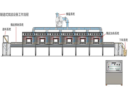
So researchers at Cornell University came up with a new way to increase the equilibrium concentration of phosphorus: the microwave process.
During the experiment, the researchers put the chips doped with phosphorus atoms into the innovative microwave oven at home and found that the microwave process could activate the doping atoms in the chip material without causing the transistor to expand.
Now James Hwang of Cornell University and Gianluca Fabi, a postdoctoral fellow, have filed two patents for microwave detractors, and the papers have been published in Applied Physics Letters.
The researchers predict that the technology will be applied to chip manufacturing by 2025.
As early as 2025, Taiwan Semiconductor Manufacturing Co., LTD. 's 2nm chips may be ready for mass production. In other words, the manufacture of 2nm chips may require a microwave device in addition to EUV lithography.